
Rothberg’s New Gadget (ii) - Is this the 'Secret Sauce'?
This is the second commentary of a series of technical posts on the miracle gadget being built by Jonathan Rothberg’s new company. For overview, readers are encouraged to go through the following introductory post.
Technical Details of Rothbergs New Machine (i)
-————————————————
Secret sauce
Recently, MIT Technical Review wrote -
Rothberg claims theres a secret sauce to Butterflys technology, but he wont reveal it.
In this commentary, we will speculate on what that ‘secret sauce’ is likely to be. It appears that the most elegant (and challenging) aspect of his new device is the marriage between MEMS and CMOS circuit technology using clever semiconductor processing steps. We will first describe each component (MEMS- CMUT and CMOS) and then explain what is needed to combine the two. Be warned that we are trying to ‘reverse engineer’ a device that is yet to be built and doing so with no help from those who are building it. Our presentation is written entirely from public data, Snowden files, Wikileaks and tapping into NSA’s global snooping network :)
-——————————————————
1. CMOS circuit technology
CMOS is a well-established technology and is at the heart of every computer chip being used today. It is done by starting from a pure semiconductor wafer and systematically building a complex circuitry on top of it through extensive use of optical masking and patterning.
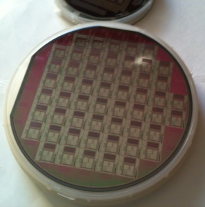
Here is a quick iphone photo of a mixed-signal test chip we used to routinely build about fifteen years back. What you see in the above image is the fully- built circuit on top of a 8” silicon wafer. If you turn around the wafer, the other side looks completely shiny (like the back of a DVD), and that is the initial material the engineers start with. Then they cover the wafer using photo-active materials, put an optical mask on it and shine light. The chemical properties of the parts receiving light change from the masked regions and
can be chemically washed away. That means parts of the silicon wafer are exposed to further processing and other parts are covered. Those parts are chemically processed and then another mask is put on to build the next layer of circuitry. Through many iterations of this basic process of photolithography, any complex circuitry can be built on top of the wafer. A simple example is shown below.
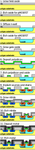
CMOS inverter -

Processing steps to build it -
-——————————————————
2. CMUT or Capacitive micromachined ultrasonic transducers
MEMS (microelectromechanical systems) is relatively new compared to CMOS and started in mid-90s. The idea was to build small mechanical devices on silicon using similar photolithography steps. Here we will only focus on one aspect of MEMS - capacitive micromachined ultrasonic transducers (CMUT).
Let us first explain the word transducer. In the CMOS circuit shown in previous section, all operations are done using electrical circuits and electric energy, but to deal with the real world, it is often needed to convert between electrical signals and other forms of energies. A transducer is a device that converts between electric signals and any other form of energy. For example, LED and miniaturized photo-receptors are good examples of transducers converting between electric energy and light.
Since most transducers are big compared to CMOS circuits on chips, they increase the sizes of actual gadgets. MEMS promises to miniaturize the transducers by using the same lithography technique as explained above. Let us see how CMUT achieves that.
Capacitive micromachined ultrasonic transducers (CMUT) is a relatively new concept in the field of ultrasonic transducers. Most of the commercial ultrasonic transducers today are based on piezoelectricity. CMUTs are the transducers where the energy transduction is due to change in capacitance. CMUTs are constructed on silicon using micromachining technique. A cavity is formed in a silicon substrate, and a thin layer suspended on the top of the cavity serves as a membrane on which a metallized layer acts an electrode, together with the silicon substrate which serves as a bottom electrode.
If an AC signal is applied across the biased electrodes, the vibrating membrane will produce ultrasonic waves in the medium of interest. In this way it works as a transmitter. On the other hand, if ultrasonic waves are applied on the membrance of biased CMUT, it will generate alternating signal as the capacitance of the CMUT is varied. In this way, it works as a receiver of ultrasonic waves.[1]
In essence, they are forming miniaturized drums in the form of small cavities, and each drum has its own resonance frequency depending on its size and shape. As you see, forming cavities on wafers involves another level of complexity, because the conventional processing does not allow for making sealed holes. Therefore, to build them, usually another wafer is placed on top of the processed wafer with cavities and two wafers are joined by a method named wafer bonding.
To learn where the state of the art regarding CMUT is, readers are encouraged to take a look at various papers from B. T. Khuri-Yakub’s group in Stanford, such as the following one from 2013.
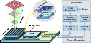
Integrated circuits for volumetric ultrasound imaging with 2-D CMUT arrays
Real-time volumetric ultrasound imaging systems require transmit and receive circuitry to generate ultrasound beams and process received echo signals. The complexity of building such a system is high due to requirement of the front- end electronics needing to be very close to the transducer. A large number of elements also need to be interfaced to the back-end system and image processing of a large dataset could affect the imaging volume rate. In this work, we present a 3-D imaging system using capacitive micromachined ultrasonic transducer (CMUT) technology that addresses many of the challenges in building such a system. We demonstrate two approaches in integrating the transducer and the front-end electronics. The transducer is a 5-MHz CMUT array with an 8 mm 8 mm aperture size. The aperture consists of 1024 elements (32 32) with an element pitch of 250 ?m. An integrated circuit (IC) consists of a transmit beamformer and receive circuitry to improve the noise performance of the overall system. The assembly was interfaced with an FPGA and a back-end system (comprising of a data acquisition system and PC). The FPGA provided the digital I/O signals for the IC and the back-end system was used to process the received RF echo data (from the IC) and reconstruct the volume image using a phased array imaging approach. Imaging experiments were performed using wire and spring targets, a ventricle model and a human prostrate. Real-time volumetric images were captured at 5 volumes per second and are presented in this paper.
Complete circuitry is shown here.
-——————————————————
Advancements in the Newly Proposed Device
Adding wires to the vibrating drums to measure their signals is the biggest challenge in scaling up the existing CMUT method. Each drum needs to have its own connector and that means ~1000 wires to control/measure a 32x32 CMUT device.
The newly proposed device solves this problem and the solution (‘secret sauce’) is to add contacts from the bottom wafer by using metallization through via holes, just like it is done in the CMOS circuitry. Here is a picture from their patent application -
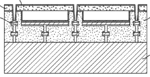
In other words, the transducer array becomes another component just like CMOS transistors in a large integrated circuit and is built together with the remaining circuitry through lithography-based processing steps. One critical difference - conventional CMOS does not add another wafer on top through wafer bonding, but that step is needed here to make sealed cavities as tranducers. The company proposes a set of steps to make cavities in a wafer with fully- built CMOS circuitry and then add second wafer on top. The second wafer will form a amorphous silicon/polysilicon membrane to cover the cavities.
What are the challenges?
1. bonding -
To make sure the metal layers (interconnects) in the lower level do not get damaged while the second wafer is bonded, all processing steps on top of it need to be done at below 450C. Therefore, they plan to bond the second wafer using fusion bonding or adhesive-based bonding.
2. Interconnecting the cavities -
Once the top wafer is placed, will it be easy to identify the locations of the cavities and connect them to the bottom wafer by metallic junctions linked to the via holes? How small can the cavities be to ensure that this metallization scheme continues to work accurately? We do not have an answer to this question.
-——————————————————
How Revolutionary is the entire device?
To understand how revolutionary the above achievement can be, readers may take a look at a prior example of combining CMOS electrical circuitry with another form of energy - light. There is no doubt that digital cameras came out of nowhere about fifteen years back and completely revolutionized the world of photography. At the heart of many digital cameras is another energy-conversion device known as CCD or charge-coupled device.
The photoactive region of a CCD is, generally, an epitaxial layer of silicon. It is lightly p doped (usually with boron) and is grown upon a substrate material, often p++. In buried-channel devices, the type of design utilized in most modern CCDs, certain areas of the surface of the silicon are ion implanted with phosphorus, giving them an n-doped designation. This region defines the channel in which the photogenerated charge packets will travel. Simon Sze details the advantages of a buried-channel device:[15]
This thin layer (= 0.20.3 nm) is fully depleted and the accumulated photogenerated charge is kept away from the surface. This structure has the advantages of higher transfer efficiency and lower dark current, from reduced surface recombination. The penalty is smaller charge capacity, by a factor of 23 compared to the surface-channel CCD.
We mention the CCD example to also explain the business challenges in building transducer-coupled digital circuitry. It took many years to integrate CCDs with CMOS circuitry, but CCDs used too much electricity and made users recharge their cameras often. This was not a popular option, and a new class of CMOS sensors turned out to be the winners.
CMOS Is Winning the Camera Sensor Battle, and Here’s Why
As a result, the companies that first entered the market were not the most successful ones.
-——————————————————
**Operational Details - Are they Doing CMOS in-house or as fabless? **
After going through the processing steps, the question that popped in our mind was whether the company would build the CMOS circuitry (lower layer) in-house or in a fabless setup. The advantage of going fabless is to be able to get very high density and thus do a lot more analysis in the chip. On the other hand, the new MEMS processing steps being introduced for forming sealed cavities are hard to get done outside and are more likely being done in-house. Therefore, a fully processed VLSI wafer needs to be brought in house to build additional layers.
Based on our understanding, the lower layer is more likely to get done in house and definitely not at a high-density shop like TSMC. We may be wrong on this, but the major implication of above difference is that the CMOS circuitry in the chip will most likely only contain essential analog/mixed-signal processing steps and maybe simple blocks like MUX, but the bulk of the signal reconstruction analysis has to be done in an external unit like an FPGA. We will discuss the circuitry in a follow-up commentary, where these issues will be covered.